“Happy Accident” Uncovers New Transport Process of Atoms in 2D Spaces
Researchers from Princeton Chemistry and Princeton Physics have discovered a surprising process that rapidly and uniformly disperses palladium and other metals over a confined, two dimensional space at a temperature far below its melting point.
The transport process also creates a stable new 2D crystalline material from the base metal palladium and the parent crystal. The resulting compounds are only a few atoms thick and were previously not known to exist.
During experiments, the material uniformly blooms across the obtaining surface in defiance of well-known laws of diffusion; almost, scientists say, the way spilled ink saturates a piece of paper – except there are no liquids involved.
And they have no idea why.
As they seek to explain this phenomenon and explore applications of the new compounds, researchers extoll the simplicity of this generalizable process that could have exciting implications for the synthesis of 2D materials and for unlocking new device functionalities.
The paper, Surface-Confined Two Dimensional Mass Transport and Crystal Growth on a Monolayer, was published jointly by Associate Professor of Chemistry Leslie Schoop and Assistant Professor of Physics Sanfeng Wu in Nature Synthesis this week.
“This is not only a new way of making 2D materials, it is making materials that we don’t even have yet,” said Schoop. “There are other types of 2D materials, but they’re almost all made from 3D materials out of bulk. What we’ve found is that we can make 2D materials with this new method that don’t have analogs. They’re completely new. We don’t even know what they can do yet.
“This method is so simple,” she added. “You put a flake of 2D material down and a little bit of metal on top of it and then you put it on a hotplate, and the metal disperses really quickly, covering the entire surface. The metal would normally melt at a 1000 degrees C, but here it happens at about 200 degrees C. This could be done at your electric stove.”
“When we study a 2D crystal, the first assumption is that this is the material we want, and we hope not to change it,” said Wu. “We do everything to protect that from happening. But this discovery immediately tells us that, there is a whole new world if we change our mind.
“There are many questions to be addressed regarding how atom transport and chemical reactions occur in spatially confined nanoscale systems that are crucial to fields like nanotechnologies, molecular biology, and quantum material science. Our experiments reveal that, even in the simplest format, where an elemental metal interacts with a single atomic layer of a crystal on its atomic plane, it is full of surprises.”
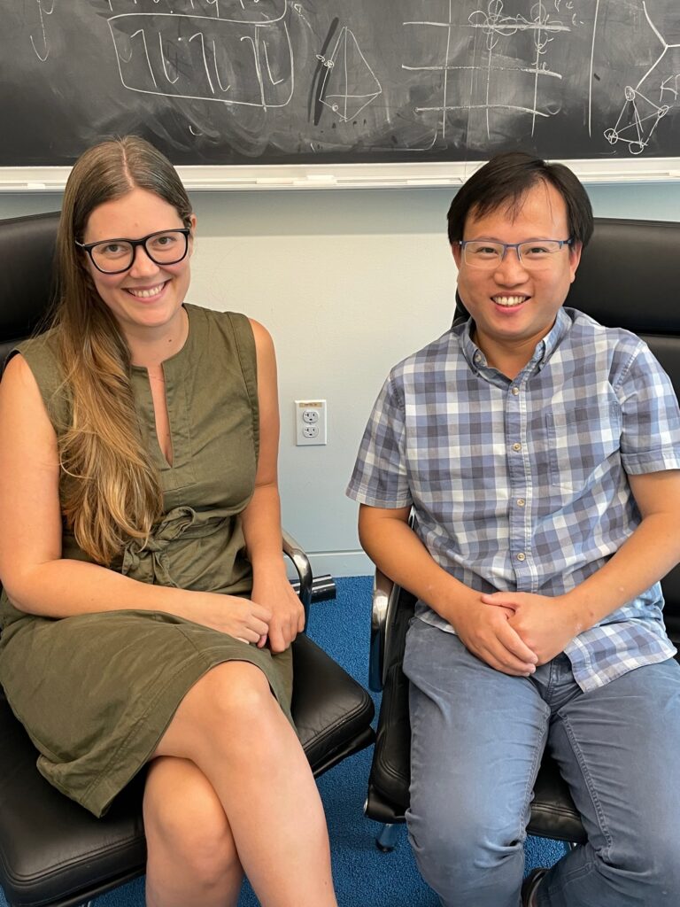
Associate Professor of Chemistry Leslie Schoop and Assistant Professor of Physics Sanfeng Wu publish on an unusual transport and crystal growth process and its resulting new 2D materials, discovered in their labs.
Wu has long collaborated with Schoop to explore and characterize atomically thin quantum materials, and together they have published several important papers. But this one, said Wu, takes the prize for its altogether unintended results.
Researchers placed a monolayer flake of tungsten ditelluride (WTe2) on top of a palladium seed island and encapsulated the sample. Upon heating it to 200 degrees Celsius, they observed something flowing from the palladium seed until it covered the entire flake.
This process of rapid mass transport goes against the convention of Fick’s laws, which describe the diffusion of atomic species into another material. The non-Fickian mass transport Schoop and Wu demonstrated delivers an atomically uniform film in the plane, crystallizing into a very specific thickness of seven palladium atoms. This is another puzzling aspect of the experiments that awaits an explanation.
Finally, this mass transport process can be turned off and on just by changing the temperature.
How They Did It
Normally, the tungsten ditelluride crystals that Schoop provides to the Wu Lab are kept at low temperatures throughout the fabrication process. That is standard procedure. But in this case, Yanyu Jia, a graduate student in the Wu Lab, heated the material up slightly. It was immediately apparent that something unusual was happening.
“This was a happy accident during a long project,” said Jia. “One late night, on the verge of giving up on that project that had consumed a year of my life, I decided to break that rule that you never overheat the device. Almost immediately, I observed something unusual. Something began to propagate from the metal contact into the 2D materials of our device. My initial reaction was one of utter confusion. This was an entirely unprecedented phenomenon.”
So far, researchers have found that the process works with both palladium and nickel, but not with gold.
The method has already found its first application in a paper also out of the Schoop and Wu Labs published in the journal Nano Letters this summer. In that investigation, Schoop Lab postdoc Fang Yuan and Jia used this palladium transport approach as a “glue” to fix air-sensitive 2D crystals during transmission electron microscopy (TEM).
“This enhanced adhesion proved crucial in preparing TEM samples, including the monolayer and twisted bilayer samples obtained through mechanical exfoliation and fabrication,” said Yuan. “Building on these discoveries, we have successfully developed a step-by-step methodology for obtaining atomic-resolution TEM images of the highly air-sensitive monolayer and twist bilayer WTe2.”
Much remains to be investigated, said Schoop. But the prospects are exciting.
“I think this is the dream of every child who wants to be a scientist,” Schoop said. “You hope that you discover something completely new where you’re saying, what the heck is going on here? This is one of those moments.”
Added Wu, “We are applying the approach for creating quantum structures and devices that were hard to imagine before. Right now, this is an accident that solves several problems all at once.”
Leslie Schoop and Sanfeng Wu would like to acknowledge funding, grants, and services in support of this research from the Office of Naval Research, the National Science Foundation, the Air Force Office of Scientific Research, the Eric and Wendy Schmidt Transformative Technology Fund, the Gordon and Betty Moore Foundation, the David and Lucile Packard Foundation and the Sloan Foundation, and the Imaging and Analysis Center at the Princeton Materials Institute.