Kunin investigates new generation of semiconductors on PPPL-led project
A new multidisciplinary project that aims to expand America’s competitive edge in semiconductors is underway through the U.S. Department of Energy’s (DOE) Princeton Plasma Physics Lab and faculty members across campus, including Princeton Chemistry’s Alice Kunin.
The DOE has funded the project to support research developing new types of two-dimensional semiconductors by porting over lessons from the traditional toolkit already in use for processing 3D semiconductors. Semiconductors are the foundation of the memory, storage, and processing power used in commercial, industrial, and military-grade devices.
As innovation drives electronics ever smaller and thinner, we are reaching the limits of their processing capabilities. This is particularly true for silicon, the standard foundational material for microchip transistors.
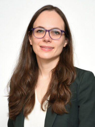
Alice Kunin, assistant professor in the Department of Chemistry.
The four-year project will focus on the use of a new family of materials called transition metal dichalcogenides. These materials are semiconductors with a crystal repeating structure and unique properties that researchers believe they can exploit for next-generation electronics.
“There’s an interest in the electronics community to try to pack as many transistors on any given chip as you possibly can to increase the density. That means that each individual transistor needs to be made smaller and smaller to enable a smaller computing form factor or increase the computing capability,” said Kunin, assistant professor in the Department of Chemistry, who did research as a postdoctoral fellow on semiconductors that can be thinned down to individual monolayers.
“One of the challenges in the community from a microelectronics perspective is that we’re reaching the limit of how small and thin electronics can be made and still maintain their microprocessing capabilities. When you start to make electronics very, very small, you reach a limit where it becomes difficult to control the behavior of the electrons in the way that you want.”
Together with other investigators, Kunin will work on a toolbox enabling the integration of these 2D materials into next-generation semiconductor device manufacturing.
Plasma-based processing
This is one of two highly competitive Microelectronics Science Research Center projects announced by PPPL in December. It will be led by PPPL Principal Investigator/Director Yevgeny Raitses and Co-Principal Investigator/Co-Director Barry Rand, professor of Electrical and Computer Engineering and a PPPL associated faculty, with academic and industry partners in Houston, Michigan, New York, and California.
Kunin is eager to investigate the properties of transition metal dichalcogenides, atomically thin semiconductors. For one thing, she said, they interact with visible or infrared light, making them of interest for a wide range of electronic devices. For another, their light-interaction properties differ between the material’s monolayer form and its bulk form, creating opportunities to tune the properties by modifying the number of layers or by combining different monolayers together in one device.

An artist’s representation of a hole etched into alternating layers of silicon oxide and silicon nitride using plasma, which is used to make 3D NAND flash memory.
Kunin will work with ECE Assistant Professor Saien Xie, whose lab specializes in growing large-area, high-quality monolayer materials.
“That’s one major advance that’s taking the first step towards enabling these materials to go from demonstrating exotic physics to actually being used for electronics,” said Kunin. “Once you can make these in a homogenous wafer-scale size, then you can really start to do processing.
“The other piece of the puzzle this project will address is that a large proportion of all the processing we do for making electronics is plasma-based processing. That’s a lot of what we use for enabling thin film deposition or controlled thin film removal such as cleaning or etching. Electronic devices are typically comprised of multiple layered or interconnected material components that make up the total device architecture. Plasma-based processing is a very powerful approach used for enabling that layered fabrication process.”
PPPL collaborates with the semiconductor industry, academic institutions and the DOE lab complex to develop better ways to make next-generation materials and manufacturing processes for computer chips, memory, and sensors. The lab’s expertise in low-temperature plasmas, which are used in nearly half of all semiconductor fabrication steps, makes it the ideal entity to lead this project.
Researchers know how to use plasmas to do traditional 3D semiconductor processing. Now, they will develop a knowledge base for how plasmas interact with these new types of 2D materials and, beyond that, how to process them for use with electronic devices.
“After Saien grows these materials, my group has the expertise to characterize them and look at them either optically or with other types of spectroscopies so we can see what’s happened to the material structurally, what was the effect of the interaction with different plasma conditions, and how we have changed the way these materials interact with light or their overall electronic properties.”
The industry partner on this project is IBM’s Thomas J. Watson Research Center in New York, which Kunin said will give her lab members valuable experience interacting directly with industry-based researchers.